
Electroless Nickel Plating for Mold Surfaces: When It Beats PVD
Table of Contents
A 32-cavity connector mold built to ±0.005 mm comes off an 180,000-shot PVC program with rust blooming inside the core-side cooling channels and a cavity that drags on release. Hard chrome would have shielded that cavity steel from the hydrogen chloride the resin releases. No chrome anode reaches 90 mm down a Ø6 mm core pin bore, though, so the bore rusts while the cavity face is protected. The tool goes out for stripping and re-polishing, and the cell loses 11 days.
The same gap appears on short runs. A flame-retardant PBT program at 40,000 shots etches a matte band across the gate area of a polished S136 insert because the halogenated additive attacks the steel surface. A PVD coating would protect that band, but the 600 kg insert will not fit a coating chamber without splitting the tool. Two corrosion problems, two surface treatments, each the wrong shape for the job.
Electroless nickel plating fills that gap. It is an autocatalytic nickel-phosphorus deposit that needs no current path, so it covers deep cavities, blind holes, internal water channels and the bores that hold core pins. It plates at 85-95°C, so hardened mold steel at HRC 48-62 keeps its heat treatment. It costs a fraction of a PVD coating per tool. This guide is written for mold buyers and tooling engineers deciding between electroless nickel, hard chrome, PVD, DLC and nitriding. Hardness, thickness, corrosion and cost figures below are typical published values for production plating.
The Snapshot
- Electroless nickel (EN) is an autocatalytic Ni-P deposit with no current path. Thickness holds within ±10 percent across a part and reaches blind holes and internal channels where both electroplated chrome and line-of-sight PVD fail.
- Typical mold builds run 5-25 µm per surface, and 25-50 µm for corrosive service. Both sides of a shut-off grow by the full thickness, so a 25 µm build adds 0.05 mm to a pin diameter.
- Medium phosphorus (5-9 percent P per ISO 4527) is the mold default at 500-600 HV as-plated. High phosphorus (10-13 percent P) gives up hardness for corrosion resistance and passes 500-1,000 hours of ASTM B117 salt spray at 25 µm.
- Against 30-40 percent glass-filled resin, EN at 500-600 HV wears faster than PVD or DLC at 2,000-3,000 HV. EN wins on corrosion, release, uniformity, internal reach and cost per tool.
- Adhesion is a process variable, not a coating property. A 190-220°C hydrogen relief bake inside 4 hours of plating and an ASTM B571 thermal shock test are what separate a 5-year deposit from one that blisters at 20,000 shots.
Why Mold Surfaces Fail Before the Steel Does
Mold steel is usually the strongest link in the decision chain and the last thing to fail. A 1.2343 or S136 cavity at HRC 48-52 carries 500-1,200 bar of injection pressure for millions of cycles, and the bulk material rarely gives up first. The surface does. Three modes account for most premature surface damage on a tool: chemical attack from the resin, adhesion of polymer to steel, and abrasive wear from fillers.
Chemical attack is corrosion, and it is the mode most often misdiagnosed as wear. PVC releases hydrogen chloride above 180°C, and moisture in the melt turns that gas into hydrochloric acid. Flame-retardant grades of PBT, PPS and PA break down into acidic species. Condensate in a water-cooled core with a pH below 6 pits bare steel at 5-20 µm per year in a lightly protected circuit. A mold surface that corrodes does not only look dull. It loses its polish, holds the part harder and drags during ejection.
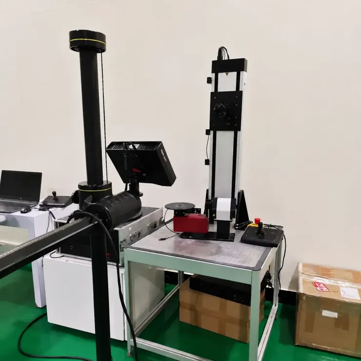
Release is the second mode and it is mechanical rather than cosmetic. Polymer sticks to steel when surface energy is high and micro-texture gives the resin a mechanical key. Polished S136 at Ra 0.05 µm releases cleanly. The same surface after 300,000 shots, with micro-scratches and a partly oxidized oxide layer, holds the part at the gate and at the ejector pads. Ejection force rises 20-40 percent, pin marks appear and thin-wall parts warp.
Wear is the third mode, and it is the one that pushes most shops toward PVD. Glass fibers at 30-40 percent loading act like a lapping compound. Gate lands erode, ejector pin bore clearance opens from 0.02 mm to 0.05 mm, and the tool starts flashing. Abrasion rewards hardness and coating thickness, which is exactly where electroless nickel is weakest and PVD or DLC is strongest. Corrosion and release reward uniformity and coverage, which is where EN is strongest.
What Electroless Nickel Plating Is
Electroless nickel is a nickel-phosphorus alloy deposited from an aqueous bath without electrical current. Sodium hypophosphite reduces the nickel ion on any catalytically active surface in the tank, and the reaction continues as long as the part stays in solution with fresh nickel available. Mold grades run at 85-95°C and pH 4.5-5.0. That autocatalytic chemistry is what separates EN from electroplated nickel and chrome.
The missing current path is the technical reason EN wins on complex geometry. Electroplated chrome follows current density, and current density falls off with depth inside a hole while concentrating at external edges. In a Ø6 mm bore, a chrome deposit is effectively absent beyond 20-30 mm of depth and 2-3x nominal thickness on the rim. EN deposits at the same rate on a cavity face, the floor of a 90 mm core pin bore, a water channel wall and an O-ring groove. A uniformity guarantee of ±10 percent across a part is normal at a competent plating shop, and it is measured with a micrometer and a coupon, not assumed.
Typical mold builds are 5-25 µm per surface, with 25-50 µm for corrosive service and internal water channels. Deposition runs at 10-25 µm per hour, so a 25 µm build means one to two and a half hours in the bath. Every coated surface grows by the full thickness. A Ø10.000 mm core pin coated at 25 µm per side becomes Ø10.050 mm, and two mating shut-off faces close by 0.05 mm. That single number drives the pre-plate machining allowance and it is the most common source of a scrapped batch at the plater.
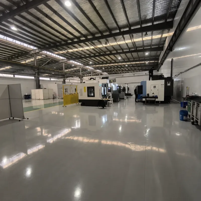
Substrate preparation decides the outcome more than the coating specification. Hardened tool steel at HRC 48-62 plates directly after alkaline clean, acid activation and a nickel strike. Aluminum needs a double zincate cycle to replace the oxide with a zinc film. Stainless needs a Wood's nickel strike to break the passive layer. Beryllium copper needs specific activation because of its beryllium oxide skin. A plater who skips the zincate on an aluminum core ships a deposit that passes visual inspection and fails a thermal shock test.
Two variants show up on mold RFQs. Composite EN carries 15-25 percent PTFE or boron nitride in the deposit and drops friction from roughly 0.40 to 0.10-0.20, which is the grade used on ejector pins and slides where release force matters. Heat-treated EN is baked at 380-400°C for one hour and reaches 900-1,000 HV, but that bake sits above the tempering range of H13, SKD61 and S136 at HRC 48-52. On those steels, coating hardness is a trade against substrate softening, not a free upgrade.
Medium vs High Phosphorus EN
Phosphorus content is the first line on an EN specification and it changes almost everything about the deposit. ISO 4527 and ASTM B733 split the range into three working bands. Low phosphorus is 1-4 percent P, medium is 5-9 percent P and high is 10-13 percent P. Two deposits at the same 25 µm thickness behave like different materials in service.
Low phosphorus is crystalline, magnetic and the hardest of the three as-plated at 700-750 HV, and it responds to a 400°C bake by climbing to 1,000-1,100 HV. It is also the most corrosion-prone grade, because the crystalline structure gives electrolyte grain boundaries to follow. Low-P is a wear coating. It shows up in hydraulic rods and textile machinery more than in molds.
Medium phosphorus is the mold default. As-plated hardness is 500-600 HV, roughly HRC 49-52. The structure is mixed amorphous and microcrystalline, internal stress is low, and the deposit tolerates a 190-220°C hydrogen relief bake without losing hardness. It releases most unfilled and lightly filled resins cleanly and holds up on sliding fits. Where a tool needs reliable release with moderate wear resistance, medium-P at 15-25 µm is the standard answer.
High phosphorus is chemically the strongest option. Above roughly 10 percent P the deposit becomes essentially amorphous, with no grain boundaries for a corrosive medium to follow. A 25 µm high-P layer on steel typically passes 500-1,000 hours of ASTM B117 salt spray before the first red rust, against 100-300 hours for a comparable medium-P deposit and under 100 hours for porous hard chrome. High-P is also non-magnetic, which matters for electronics tooling. The cost is hardness at 480-550 HV as-plated and price at 20-40 percent above medium-P, because the bath is harder to control and the chemistry is dearer.
The practical split for a mold shop is simple. Medium-P for general injection tooling, ejector components and slides where release and moderate wear resistance are the drivers. High-P for PVC and halogenated flame-retardant resins, for water-cooled channels where condensate pits bare steel, for blow molds, and for food-contact tooling where lead-free chemistry is specified. Legacy lead-stabilized baths still exist, so a food or medical program should ask for an elemental analysis rather than a verbal assurance.
EN vs Hard Chrome vs PVD
Hard chrome, PVD and EN overlap in the middle of the performance map and diverge at the edges. Chrome is an electrodeposit that builds fast and hard but throws poorly. PVD is a vacuum deposit that is line-of-sight, very hard and thin. EN is a chemical deposit that trades peak hardness for uniformity, corrosion resistance and reach. The table below is the reference card for the three, plus the high-phosphorus EN grade that behaves differently enough to deserve its own column.
| Property | EN medium-P (5-9%) | EN high-P (10-13%) | Hard chrome | PVD (TiN, CrN, DLC) |
|---|---|---|---|---|
| Deposit type | Autocatalytic Ni-P | Autocatalytic Ni-P, amorphous | Electroplated Cr | Vacuum arc or sputter |
| Typical thickness | 5-25 µm | 25-50 µm | 10-50 µm | 1-5 µm |
| Hardness as applied | 500-600 HV | 480-550 HV | 800-1,000 HV | 2,000-3,000 HV |
| Thickness uniformity | ±10 percent, all surfaces | ±10 percent, all surfaces | Edge build 2-3x, holes starved | Line-of-sight only |
| Internal bores and channels | Fully coated | Fully coated | 20-30 mm depth limit | Not coatable |
| ASTM B117 salt spray at 25 µm | 100-300 h to red rust | 500-1,000 h to red rust | Under 100 h, porous | Substrate-dependent, pinholes |
| Friction against steel | 0.35-0.45 | 0.35-0.45 | 0.30-0.40 | TiN 0.4, DLC 0.05-0.15 |
| Max continuous service temp | 250-300°C | 250-300°C | 300-400°C | TiAlN to 800°C, DLC to 350°C |
| Masking and stripping | Minimal masking, strip and re-plate | Minimal masking, chemical strip | Heavy masking, hard to strip | Careful masking, chemical strip |
| Part size fit | Tank size, up to 1-2 m parts | Tank size | Tank size | Chamber 1,000-1,500 mm typical |
| Typical cost per small component | $25-150 per batch | 20-40 percent above medium-P | 20-40 percent below medium-P | $150-600 per tool set |
| Main failure mode | Abrasive wear, impact spalling | Abrasive wear, poor adhesion if prepped badly | Cracking, porosity, edge flaking | Thin film wear-through, cost |
← swipe to scroll →
Table note: hardness, thickness, salt spray and cost values are typical industry figures for production plating. Actual results depend on substrate, bath chemistry, pretreatment and part geometry, so every specification should carry a coupon test or a batch certificate.
Two operational differences sit behind the table and decide most projects. Chrome and PVD both need a tank or a chamber that the part fits into. A 600 kg cavity insert with a 400 mm water jacket will not go into a PVD chamber without splitting the tool, and it cannot be masked affordably for chrome. EN plates into the assembled geometry, so an insert that arrives as a finished component comes back with every internal surface coated, including the water circuit.
Cost per tool is the second difference. A plating quote for small mold components typically runs $25-150 per batch at medium-P thickness, hard chrome commonly lands 20-40 percent below that, and a full PVD tool set with masking and re-polishing runs $150-600 per tool. Those figures swing with part size, so the useful comparison for a program decision is cost per protected surface and cost per avoided day of downtime, not cost per part.
Where EN Wins: Deep Cavities and Internal Surfaces
Uniformity is the reason to choose EN, and it shows up in four geometries that dominate precision tooling. Deep cores and narrow ribs come first. A connector mold with 8 mm tall ribs at 0.9 mm width has a depth-to-width ratio of about 9, and a PVD source cannot line-of-sight a metal vapor into that slot. EN reaches it because the deposit grows chemically on every wetted surface, and plating solution circulates through a 0.9 mm slot with normal bath agitation up to a depth-to-width ratio of roughly 10 before flow starvation starts to thin the deposit.
Deep core pin bores come second. A Ø3 mm bore, 45 mm deep, machined to hold a core pin at HRC 60, is a corrosion trap in a water-adjacent environment. Hard chrome puts 0 mm on the floor of that bore and 2-3x nominal on the entry chamfer. PVD cannot coat it at all. EN at 12-15 µm covers the full 45 mm length, and a coupon cut from a witness pin verifies it. Internal water channels show the same advantage. A Ø8 mm channel drilled 400 mm through a mold base can be plated at 10-15 µm on the wall, which converts a rusting passage into a stable one for a modest reduction in flow area of under 1 percent.
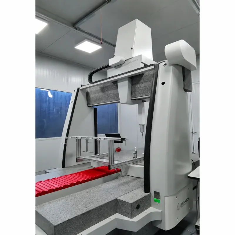
Large and assembled geometry is the fourth case. PVD chambers typically handle parts up to 1,000-1,500 mm, and tool size falls out of the process on anything larger or heavier. A plating tank has no comparable limit, and EN needs no anode placement, so a finished mold base section with a water jacket, ejector holes and leader pin bores goes into the bath as one piece. Masking is limited to threads and surfaces that must stay conductive or fit-critical, which is a fraction of the masking a chrome job requires on the same part.
There is a limit worth knowing. Below roughly 1 mm of slot width or 3 mm of bore diameter, solution exchange inside a long channel becomes the controlling variable, and deposit thickness can drop 20-30 percent at the deepest point. Platers handle it with higher bath circulation, part rotation, or a lower build target with a longer dwell. The point is to raise the geometry before quoting, not after the coating comes back thin at the far end of a 200 mm channel.
Thickness and Dimensional Compensation
Every EN build is a dimensional decision, and it has to be made at the design stage. The coating grows outward from the surface at the full thickness, so a 25 µm build adds 25 µm per side, 50 µm on a diameter, and 50 µm across a mating pair of shut-off faces. On a mold held to ±0.005 mm, that is ten times the tolerance on a single surface. The arithmetic is simple, and skipping it is what sends a finished insert back to be stripped.
The working practice is to machine undersize by 2x the coating thickness on every coated fit and to state the pre-plate dimensions on the drawing. A Ø6.000 mm core pin at 18 µm per side is machined to Ø5.964 mm before plating and measures Ø6.000 mm after. Coating thickness control is typically ±10 percent, so 18 µm lands between 16.2 and 19.8 µm and the finished pin holds Ø6.000 mm ±0.004 mm. That is inside normal mold tolerance, but only when the plater is given the pre-plate nominal and a coupon requirement rather than a verbal 18 µm.
Sliding fits need a separate rule because both surfaces move. A core pin and its bore are normally specified at 0.01-0.02 mm diametral clearance for venting and resin exclusion. Coating both surfaces at 20 µm consumes 0.08 mm of that clearance and creates an interference fit. The practical options are to coat the pin and leave the bore bare, to coat the bore and grind the pin to match, or to coat both and pre-machine the pair to the plated nominal. The first option is the most common and the cheapest, and it keeps the bore as a ready-made touch-up surface for later repair.
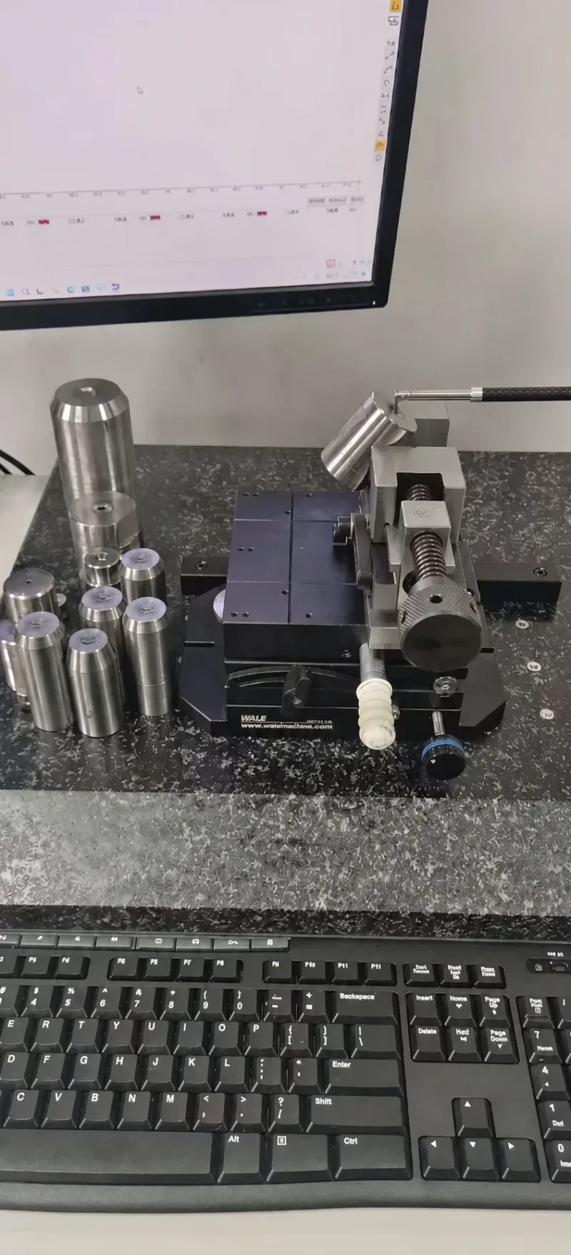
Where a fit must be held tighter than the coating tolerance allows, the sequence changes rather than the coating. Plate first, then finish-machine or lap the coated surface to nominal, or plate after final grinding with a build that sits inside the tolerance budget. EN can be ground and lapped, and a 5-10 µm coating on a polished cavity face finishes with light diamond work without breaking through. Plating is not a substitute for a dimension that was already out of tolerance.
Heavier builds serve a different purpose. Where a worn bore or a damaged boss needs restoring, EN at 50-100 µm can rebuild a surface, and the limit is internal stress rather than the bath. Deposits above roughly 75 µm in one layer carry more stress and are more prone to blistering, so a plater will usually apply a 50 µm build in two stages with an intermediate rinse. For critical fits, plating to restore is a repair tool, and it belongs with the mold repair and maintenance route, not with a new-build drawing.
Adhesion, Peeling and Blistering
Peeling is the failure that discredits EN in a mold shop, and it is almost never the coating's fault. The deposit has excellent adhesion to properly prepared steel, typically above 300 MPa in tensile pull testing on tool steel with no failure at the interface. Failures cluster in four places: contaminated surfaces, passivated substrates, unbaked high-strength steel and over-thick single-layer builds. Each has a process fix.
Contamination is the most common cause. Silicone release agents, cutting oil, EDM fluid residue and fingerprint films all survive a normal alkaline clean if they are not removed mechanically first. A part that arrives at the plater straight off a wire EDM with a sulfide-stained recast layer is a blister waiting for a load cycle. Best practice is a light polish or abrasive blast, an alkaline soak clean, an acid activation for 30-60 seconds and a nickel strike before the build. Platers who skip the strike to save a step produce deposits that pass a visual check and fail a thermal shock test.
High-strength steel adds a hydrogen risk on top of the cleanliness rule. Hydrogen absorbed during plating gathers at high-stress points and can crack hardened steel under load. The control is a hydrogen relief bake at 190-220°C for three to four hours, started within four hours of plating, which is standard practice for steel above roughly HRC 40 or 1,200 MPa tensile. A mold insert at HRC 52 that skips the bake can fail on the fourth day of production with a crack that starts a millimeter under the surface.
Verification is what keeps the process honest, and it is cheap. ASTM B571 covers standard adhesion tests for electrodeposited and autocatalytic coatings, and a thermal shock cycle from 200-250°C into water is the practical field test for mold components. Batch documentation should include a phosphorus analysis, a coating thickness reading on a coupon, a salt spray result and the bake record. A plating shop that cannot produce those four records for a given batch is a risk to the tool regardless of the price per part.
When EN Loses to PVD, DLC or Nitriding
There are four cases where EN is the wrong answer, and recognizing them early saves a coating cycle. The first is heavy abrasion from a glass or mineral-filled compound. A 500-600 HV layer 25 µm thick on an EN-plated gate land typically shows wear-through inside 150,000-300,000 shots in a 35 percent glass-filled PA66 program, while TiN, TiAlN or DLC at 2,000-3,000 HV lasts two to five times longer in the same position. Where glass loading is the dominant wear mechanism, the surface specification should start with PVD or DLC, and the design discussion belongs with the glass-filled resin tooling rules.
Hot service is the second case. EN holds up to roughly 250-300°C continuous. Above that the deposit begins to crystallize and loses both hardness and corrosion resistance, which rules it out of aluminum die casting at 600-700°C melt temperature and out of high-temperature engineering resin programs where mold surfaces run above 300°C. Nitriding builds a 0.2-0.5 mm diffused case that carries load at those temperatures, and PVD TiAlN holds to 800°C. The discussion of the trade-offs between a diffusion case and a vacuum coating is covered in the comparison of nitriding versus PVD coatings.
Impact loading is the third case. EN is a hard, relatively brittle layer on a soft or moderately hard substrate, and a stamping punch striking at 200-800 strokes per minute applies shear that spalls a 20 µm coating within a few thousand hits. Thick CVD coatings and nitrided surfaces handle impact and fatigue better, and for dies and punches the surface choice follows the steel and the die design rather than the release properties.
Friction-critical applications are the fourth case. If the objective is the lowest possible ejection force on a deep-draw part or a sticky elastomer, DLC at 0.05-0.15 friction beats EN at 0.35-0.45 and beats composite EN at 0.10-0.20. Composite EN remains the cost-effective middle option when sliding distances are short and the loads are moderate. The detailed wear and friction case for diamond-like carbon is in the guide to DLC coating for mold components.
Food, Medical and Corrosion Compliance
Compliance for a plated mold surface is about chemistry and about what the coating does under cleaning cycles, not about the color of the deposit. The corrosion baseline is the salt spray result from ASTM B117 testing. A 25 µm high-phosphorus deposit on tool steel typically reaches 500-1,000 hours before the first red rust, which is the figure to write into a specification when a mold runs halogenated resins or sits in a humid plant. Medium phosphorus at the same thickness lands at 100-300 hours and is sufficient for most unfilled resin programs.
Food-contact tooling adds two requirements. The governing frameworks are FDA 21 CFR 175.300 for food-contact coatings in the US and EU regulation 1935/2004 with 10/2011 for materials intended to contact food in Europe, alongside NSF/ANSI 51 for food equipment materials. The practical item to control is the bath chemistry: specify lead-free and cadmium-free stabilizers, and ask for an elemental analysis of the deposit rather than a certificate of conformity for the tank. Older EN formulations used lead as a stabilizer and those baths are still in service, so the question is worth asking on every food program.
Medical tooling leans on the same chemistry with two additions. Sterilization is not a problem for EN, because steam autoclave cycles at 121-134°C sit well under the 250-300°C service limit and gamma sterilization at 25-40 kGy does not degrade the deposit. What matters far more is adhesion integrity. A coated surface that blisters sheds nickel-rich particles into a cleanroom, and that is a contamination event rather than a wear problem. Any tooling for a regulated medical program should carry per-batch adhesion testing, and the program's own validation route governs the final decision on surface finish and material release.
Chemical resistance follows the phosphorus content. High-P EN resists alkalis, salt solutions, dilute organic acids and many inorganic acids, which covers PVC's hydrogen chloride, flame-retardant additive breakdown products and the mildly acidic condensate found in cooling circuits. It is attacked by concentrated nitric acid and by strong oxidizing acids, which matters at the stripping stage rather than in service. That chemistry is convenient for maintenance, because a high-P deposit can be stripped cleanly without damaging the substrate, then re-applied after polishing.
The EN Spec Checklist for Your RFQ
A plating specification that says electroless nickel, 25 µm is incomplete, and the missing fields are the ones that decide whether the deposit survives. The list below is what belongs on the drawing or the purchase order for a mold component. Each line is verifiable, and a plater who cannot answer a line should be replaced rather than accommodated.
- Substrate and hardness. Steel grade with the heat-treated hardness, for example 1.2343 at HRC 48-50 or S136 at HRC 52. The plater uses this to set the pretreatment route and the bake requirement.
- Governing standard. Cite ASTM B733 or ISO 4527 and state the phosphorus band, for example medium phosphorus 5-9 percent P or high phosphorus 10-12 percent P.
- Thickness with the pre-plate nominal. State the finished thickness per surface and the pre-plate dimension for every coated fit, for example 18 µm per side with a pre-plate Ø5.964 mm pin.
- Coated and masked areas. Identify bores, water channels, threads and datum surfaces that must stay bare. Include a marked-up drawing rather than a text list, because masking errors are a common cause of a non-conforming batch.
- Edge preparation. All coated edges radiused to at least 0.2 mm before plating. Sharp corners concentrate coating stress and are where peeling starts.
- Post-plate bake. Hydrogen relief at 190-220°C for three to four hours within four hours of plating for any steel above roughly HRC 40. Cosmetic parts at lower hardness may use a 150°C bake for adhesion only.
- Adhesion test and acceptance criteria. ASTM B571 thermal shock from 200-250°C into water, with no blistering, peeling or flaking accepted, run on a coupon from the same batch.
- Dimensional verification. CMM or micrometer readings on the coated fits before shipment, with the ±10 percent thickness tolerance converted into the drawing tolerance on the finished part.
- Batch records. Phosphorus analysis, coupon thickness reading, salt spray result and the bake log. Four records for four process variables, all traceable to the batch number.
- Repair route. Agreed strip and re-plate procedure for the same component, so a polished-out insert can be returned to nominal without a new purchase order.
The last field is worth stating in money terms. A connector OEM running multiple tools with the same coated insert family, such as the programs at TE Connectivity, Amphenol and Luxshare, benefits more from a repeatable coating specification than from the lowest quote. A $60 plating batch that comes back 5 µm thin puts a $200,000 press cell at risk of a corrosion failure in month nine, and the record trail is what proves which batch is at fault.
FAQ
Q1. Is EN a good release coating for injection molds?
Yes, for most unfilled and lightly filled resins. Medium-phosphorus EN has a friction coefficient of 0.35-0.45 against steel and a low surface energy after polishing, which reduces sticking at gates and ejector pads. Composite EN with 15-25 percent PTFE drops friction to 0.10-0.20, which is the grade used on ejector pins and slides. For the lowest possible friction, DLC at 0.05-0.15 still wins.
Q2. How thick should electroless nickel be on a mold?
5-25 µm per surface covers general injection tooling, ejector components and slides. 25-40 µm is the range for corrosive service such as PVC, halogenated flame retardants or water-cooled channels. Deposits above roughly 75 µm in a single layer carry higher internal stress and are usually applied in stages to reduce blistering risk.
Q3. Can electroless nickel be stripped and re-applied?
Yes, and it is the main reason EN fits a maintenance plan. A high-phosphorus deposit strips chemically without touching the substrate, so an insert can be stripped, re-polished and re-plated rather than replaced. Strip and re-plate typically costs 40-60 percent of a new component, and a complete cycle usually takes 5-10 working days.
Q4. Does EN work on aluminum, copper alloy and stainless mold components?
It does, with different pretreatments. Aluminum needs a double zincate cycle, stainless needs a Wood's nickel strike to remove the passive film, and beryllium copper needs specific activation for its oxide layer. Each adds one process step and one failure mode, so those parts should carry a sample coupon requirement.
Q5. Will EN stop ejector pin wear in glass-filled resin?
Only partly. At 500-600 HV and 15-25 µm, EN improves release and corrosion resistance but does not match a 2,000-3,000 HV PVD or DLC layer against 30-40 percent glass fiber abrasion. In a 35 percent glass-filled PA66 program, expect coated pin life in the 150,000-300,000 shot range against 100,000-200,000 for uncoated SKD61 at HRC 58-60, and choose DLC when the wear mechanism dominates.
The Bottom Line
Electroless nickel plating is not the hardest coating on the quote and it is the only one that reaches internal channels, deep bores and assembled geometry at a uniform ±10 percent thickness. Specify medium phosphorus for release and general tooling, high phosphorus for corrosion, and pre-machine every coated fit by twice the build. Get the phosphorus band, the bake and the batch records on paper. DieStrike builds precision injection molds and stamping dies to ±0.005 mm and works the surface specification into the DFM stage, so the coating decision is made before the steel is cut. Send the tooling geometry and resin data through the contact form and we will return a DFM note within 24 hours.
KEEP READING
Related Reading
Nitriding vs PVD Coatings for Mold Steel: Which Surface Treatment When
Diffusion cases versus vacuum coatings on hardness, depth and cost, and how they sit against chemical nickel.
Read articleArticleDLC Coating for Mold Components: When It Pays Off
Diamond-like carbon at 2,000-3,000 HV, friction 0.05-0.15 and the wear cases where EN cannot compete.
Read articleArticleHow to Design Molds for Glass-Filled Resins: Wear, Gates and Steel
Abrasion budgets, gate land erosion and the steel and surface choices for 30-40 percent glass loading.
Read articleServiceMold Repair and Maintenance
Strip, re-polish and re-plate support from an IATF 16949 certified precision mold maker.
Read articleNEXT STEP
Ready to Start Your Mold?
Send us your element dimensions or part numbers — our team responds within 24 hours with pricing and lead time.

Written by
Ray ChanMold Buyer's Guide Author · Precision Mold Manufacturing Specialist. Ray helps global importers, distributors and OEMs source factory-direct molds and mold parts.