
EDM Surface Finish vs SPI Texture: How to Specify Both
Table of Contents
Two weeks before a T2 sample, a hardened S136 insert for a connector housing came out of sinker EDM at Ra 1.6 µm with a soft matte look nobody had asked for. The drawing carried two notes. One said SPI C-1 polish over 80% of the cavity. The other said texture on the run-out faces. The shop polished most of the cavity to Ra 0.4 µm, then re-sparked three areas to fix a weld line that the first trial exposed. The etch vendor opened the box and got an uneven result, because the re-sparked zones sat 0.8 µm rougher than the polished field around them. The tool shipped 9 days late and the finishing line on that invoice grew by 14%.
None of that delay came from bad machining. It came from a missing interface on the drawing. EDM finish and SPI texture are two separate numbering systems that meet on the same steel surface. Spark finish is quoted in VDI 3400 or Charmilles numbers by the EDM cell. Polish and texture are quoted in SPI grades by the bench and by the etch house. When a drawing names only one system, the other is filled in by assumption. Assumption is what sends a finished cavity back to the electrode.
This guide is written for mold buyers, tooling engineers, and program managers who have to put both call-outs on one drawing and get one consistent surface across a range that runs from Ra 0.012 µm to Ra 6.3 µm. It covers what a spark cut actually leaves on the steel, how the VDI, Charmilles and SPI scales convert, how much stock to leave for polish, when a texture will hide EDM marks and when it will ghost them, and what a finish house measures before it issues a report. The Ra values, layer depths and bench hours below are typical industry figures for production injection molds. Treat them as planning numbers and confirm the final targets against your own plaques and reports.
The Snapshot
- Two systems, one surface. EDM finish is quoted as VDI 3400 (0 to 45) or Charmilles (0 to 63) crater roughness. Polish and texture are quoted as SPI grades A1 to D3, where A1 is Ra 0.012 µm and C-1 is Ra 0.8 µm.
- Ra is the bridge between them. Charmilles 18 lands near Ra 0.8 µm, the nearest VDI 3400 plate is 37, and SPI C-1 is also Ra 0.8 µm. VDI 12, Charmilles 6 and SPI B3 all sit near Ra 0.4 µm.
- Every spark cut leaves a recast layer, also called the white layer. Typical depth is 2 to 10 µm after a finish cut and 25 to 50 µm after a roughing cut on hardened steel. It must be removed before any polish or etch, or it flakes and pits in service.
- Leave 0.02 to 0.05 mm of stock after the last EDM cut for polishing. A mirror grade such as SPI A2 at Ra 0.025 µm needs roughly 0.05 mm and 30 to 60 bench hours on a hardened insert.
- Texture hides EDM marks only when etch depth exceeds crater depth. Etch depth runs 0.015 to 0.08 mm, so a coarse grain near 0.05 mm masks Ra 1.6 µm easily. A fine grain near 0.015 mm over an unpolished spark finish shows the crater pattern on every part.
- Verify with two instruments. A plastic plaque is the acceptance tool for grain and gloss, and a profilometer or optical roughness meter is the acceptance tool for Ra on the steel. A plaque alone cannot separate Ra 0.5 µm from Ra 1.0 µm.
Why EDM Finish and SPI Texture Collide
A mold drawing can carry 3 finish languages at once and still be incomplete. The geometry notes quote tolerances in millimetres. The EDM call-out references a spark finish the electrode cell understands. The cosmetic note references an SPI grade the bench and the texture house understand. Each group reads its own line and leaves the interface to the others.
The EDM cell plans an electrode and a burn sequence. Roughing burns at 20 to 60 A and leaves Ra 3.2 to 6.3 µm. Semi-finish passes step down to Ra 1.6 to 2.5 µm. A finish pass with a copper or fine graphite electrode reaches Ra 0.4 to 0.8 µm. Orbiting reduces the crater depth and improves uniformity. None of that decides what the polished area will look like.
The bench works to different numbers. It reads SPI grades and grit sequences from 240 to 3000 grit, and it measures what it can see under a bench lamp. The etch house reads grain depth and a plaque number. Both groups inherit whatever the EDM cell left behind, plus whatever the previous step removed.
The cost of the collision is easy to price. A re-spark of a hardened insert costs 4 to 10 hours of machine time plus electrode wear. A re-polish after a bad etch runs 8 to 20 hours. Stripping and re-etching a tool costs 15% to 30% of the original texture line and 2 to 4 weeks of lead time. Every one of those events traces back to a line that was never written on the drawing.
What EDM Leaves on the Steel
EDM removes steel with thousands of controlled sparks. Discharge frequency runs from about 1 kHz on a roughing cut to over 200 kHz on a fine finish cut, and each spark melts a small volume of metal that is either flushed away or resolidifies. The result is a crater field rather than a cut surface, so the profile has peaks, valleys and re-melted rims instead of the directional lay that milling leaves.
Three layers sit under every burn. At the top is the recast layer, often called the white layer, produced by molten steel that cooled against the dielectric instead of being flushed away. It is 2 to 10 µm thick after a typical finish pass and 25 to 50 µm thick after a roughing pass on hardened steel such as S136 at HRC 50 or above. Under it sits a heat-affected zone where the temper has changed, usually 10 to 30 µm deep. Below that is unaffected base steel.
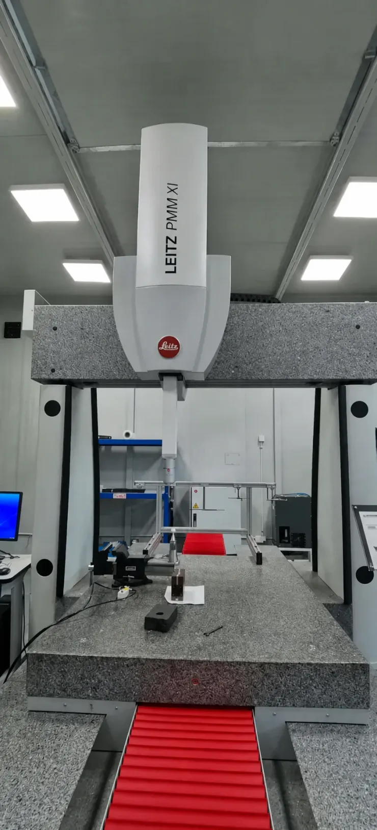
The white layer is harder than the parent steel and far more brittle. Micro-hardness inside it often reads 700 to 900 HV against roughly 500 HV in the tempered base, and it carries micro-cracks from thermal shock that can spall under load. On a polishing job that layer polishes differently from the base metal, so the bench sees a mottled surface that will not settle no matter how long the stone runs. On an etch job the acid attacks the recast layer at a different rate than the tempered steel under it, which produces blotches and an uneven grain.
Process choice changes the starting point. Wire EDM with three or four trim passes can reach Ra 0.2 to 0.4 µm with a thinner recast layer than a sinker cut, while a sinker burn is the only route into deep ribs and blind pockets. Electrode material matters too, because fine graphite and copper deliver different crater shapes at the same current. The trade-offs are covered in sinker EDM vs wire EDM and in the electrode comparison of graphite vs copper for sinker EDM.
Measurement matters at this stage. A stylus profilometer reads Ra and Rz on a 0.8 mm cutoff, which is the right setting for a molded surface. Optical or white-light instruments read the crater field without touching it and are more useful on soft or textured areas. Whichever instrument is used, the reading must be taken after the recast layer is gone, because a reading over the white layer describes a surface that will not survive the next operation.
VDI 3400 and Charmilles: Reading EDM Numbers
Two numbering systems dominate EDM finish call-outs, and they are not the same scale. VDI 3400 is a German standard that defines discrete roughness grades from 0 to 45, each tied to a reference surface. Charmilles numbers come from the EDM machine builder and run from about 0 to 63 in practical use. Both are quoted as if they were roughness, and both are converted to Ra the moment anyone has to measure.
The practical mapping is geometric. Each VDI step of about 6 points roughly doubles the Ra value, so VDI 12 near Ra 0.09 µm, VDI 24 near Ra 0.23 µm and VDI 37 near Ra 0.79 µm sit on a curve that repeats every few grades. Charmilles numbers are finer at the low end, where a Charmilles 0 sits near Ra 0.2 µm and a Charmilles 33 sits near Ra 1.6 µm. Buyers who only quote a bare number invite a mismatch, because two vendors can disagree on which chart they are reading.
| Ra target | Ra in µin | Charmilles | VDI 3400 | SPI closest | Route that gets there |
|---|---|---|---|---|---|
| 0.025 µm | 1 | below scale | below scale | A2 | EDM then diamond polish, 1 to 3 µm paste |
| 0.05 µm | 2 | below scale | 9 | A3 | EDM then 1200 to 3000 grit plus paste |
| 0.1 µm | 4 | 0 | 15 | B1 | fine EDM then 800 to 1200 grit stone |
| 0.2 µm | 8 | 0 to 1 | 24 | B2 | fine EDM then 600 grit stone |
| 0.4 µm | 16 | 6 | 30 | B3 | semi-finish EDM then 400 to 600 grit |
| 0.8 µm | 32 | 18 | 37 | C1 | finish EDM then 320 grit stone, or light etch |
| 1.6 µm | 63 | 33 | 45 | C2 | finish EDM with a light skim, or 240 grit |
| 3.2 µm | 125 | 48 | above 45 | C3 | semi-finish or roughing EDM, no polish |
← swipe to scroll →
Table note: Ra and µin columns are typical industry figures. VDI 3400 grades are discrete plates, so the nearest grade is listed. Charmilles and VDI charts drift by machine builder and by texture vendor, so confirm the mapping on the plaques that will govern acceptance.
Write the Ra number next to the scale number. A drawing that says "VDI 30, Ra 1.6 µm max" leaves far less room for interpretation than either number alone. If the surface is cosmetic, add the SPI grade and the plaque number as well, so the bench, the EDM cell and the etch house all read the same target.
SPI Finish Grades: The Polish Target
The SPI grade system is the second language on the same drawing. Grades run from A1, the optical mirror class at Ra 0.012 µm, through B and C to the textured classes in D. Each grade implies a finishing method, not just a number, because the method is what a shop quotes and schedules.
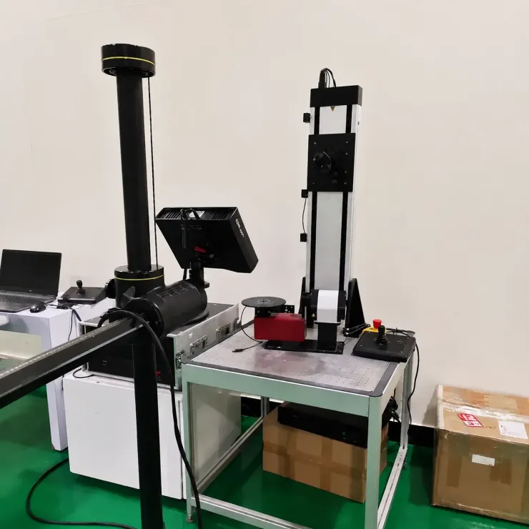
Class A covers A1 at Ra 0.012 µm, A2 at Ra 0.025 µm and A3 at Ra 0.05 µm. All three need diamond paste and a steel that can hold the finish, which in practice means a polished stainless grade such as S136 hardened to HRC 48 to 52. Class B runs B1 at Ra 0.1 µm through B3 at Ra 0.4 µm and is reached with 600 to 1200 grit stones. Class C covers C1 at Ra 0.8 µm, C2 at Ra 1.6 µm and C3 at Ra 3.2 µm, which is the everyday cosmetic range for housings and covers.
Class D and the textured classes sit at the other end and are defined by the etch rather than by the stone. A D1 surface starts from a base near Ra 0.35 µm and a D3 near Ra 0.8 µm, then the grain is added on top. The base roughness matters, because the etch reproduces the substrate. A base polished to Ra 0.2 µm etches to a cleaner, more even grain than a base that is still at Ra 0.8 µm.
The grade must match the steel. A mirror grade on a low-hardness cavity pits and scratches, and re-polishing it every 50,000 shots costs more than the steel upgrade. A 28 to 32 HRC P20 cavity can hold a good B or C finish but will fight an A grade. The mold polishing guide sets out which steel grades reach which SPI class and the grit sequence each one needs.
Etching Over an EDM Surface
Texture is applied as a photo-etched grain, and the etch does not create roughness from nothing. Depth builds in steps of roughly 1 to 3 µm per stage as the acid opens the mask. It opens what is already there. That is why the substrate condition matters more than any single etch parameter, and why an EDM surface that no one cleaned up will produce a tired, uneven grain on every part of the tool.
The arithmetic is simple enough to check before steel is cut. Etch depth for production grains runs 0.015 to 0.08 mm, with the deep end around 0.05 to 0.08 mm for coarse interior grains and the shallow end near 0.015 to 0.025 mm for fine ones. Crater depth on a spark finish follows Ra, and a surface at Ra 1.6 µm usually carries a peak-to-valley Rz near 6 to 12 µm. A 0.015 mm etch, that is 15 µm, sits uncomfortably close to a 12 µm crater depth. A 0.05 mm etch, at 50 µm, buries the crater field completely.
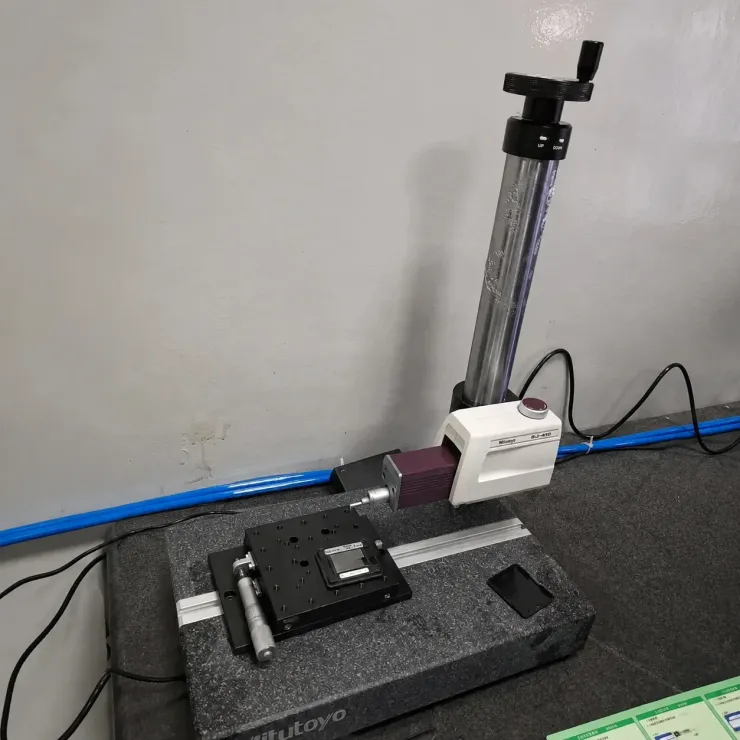
Treat a ratio of 3 to 1 as the practical floor. When etch depth is at least 3 times the crater depth of 6 to 12 µm, the grain reads as a grain and the spark pattern disappears. Below that ratio the crater pattern ghosts through as a faint orange-peel shimmer that shows up worst on high-gloss resins and light colours, and it is usually noticed after the parts are molded, not before.
Partial masking makes it worse. Many draws are half textured and half polished, with the boundary on a shut-off or a step. If the two areas arrive at the etch house 0.2 to 0.4 µm apart in Ra, the boundary reads as a hard line and the grain appears to change density along the edge. The fix is to bring the whole masked area to one uniform pre-etch finish, then let the mask define the grain. Grain, gloss, and edge control are covered in detail in how to specify mold texture.
Weld repairs and hardness variation are the other content that resurfaces after etching. A TIG or laser weld zone tempers differently from the parent steel and etches 10% to 20% deeper, so every repair spot shows as a blotch in a matte grain. Texture acceptance is a whole-surface judgement, and repair history is part of it.
Polish Stock to Leave After EDM
Polish stock is the material left for the bench to bring the surface down to grade. It is quoted in millimetres, not micrometres, because the bench has to remove the recast layer first and only then chase the grade. Under-quoting that stock is the most common reason a mold misses its finishing date. An insert that arrives at Ra 0.4 µm with 0.01 mm of stock cannot be polished to A2 without cutting into the dimensional tolerance band around it.
The working rule is straightforward. Allow 0.02 to 0.05 mm after the last EDM cut, sized to the target grade. Add 0.01 mm if the cavity has deep ribs or blind pockets where the polisher cannot reach freely with a stone holder. Add more if the EDM cell left a roughing cut unfinished, since a 25 to 50 µm white layer eats the allowance before any grade work begins.
| Target finish | Ra target | Recast to remove | Stock after EDM | Bench hours, small cavity |
|---|---|---|---|---|
| SPI A2 mirror | 0.025 µm | 2 to 10 µm plus HAZ | 0.05 mm | 30 to 60 h |
| SPI B1 to B2 | 0.1 to 0.2 µm | 2 to 10 µm | 0.03 to 0.05 mm | 10 to 25 h |
| SPI B3 to C1 | 0.4 to 0.8 µm | 2 to 10 µm | 0.02 to 0.03 mm | 4 to 10 h |
| SPI C2 to C3 | 1.6 to 3.2 µm | 2 to 10 µm | 0.01 to 0.02 mm | 1 to 4 h |
| Etched grain, D class | base 0.35 to 0.8 µm | full white layer | 0.02 to 0.03 mm before etch | 3 to 8 h plus 5 to 10 days etch |
← swipe to scroll →
Table note: stock and hour figures are typical industry values for a cavity of roughly 100 by 100 by 50 mm in hardened stainless. Scale the hours with the surface area and with the number of ribs and deep pockets.
Stock is not free the other way either. Leaving 0.15 mm instead of 0.05 mm does not make the polish easier, because the bench then has to work through a thicker layer with no gain in grade. It also risks washing out a corner radius or a shut-off land, and it changes the cavity dimension that came off the tolerance report. The dimensional consequence is real, since a precision cavity is held to ±0.005 mm on the mold and ±0.002 mm on the part geometry, and polishing is the operation most likely to quietly move those numbers.
The Surface an Etch Vendor Needs
Etch houses inspect incoming steel before they start, and they reject or flag boxes that will not etch predictably. Knowing their checklist in advance is cheaper than a rejected tool, because a flagged box costs a 2 to 5 day round trip plus a new etch slot, and the tool sits idle for all of it.
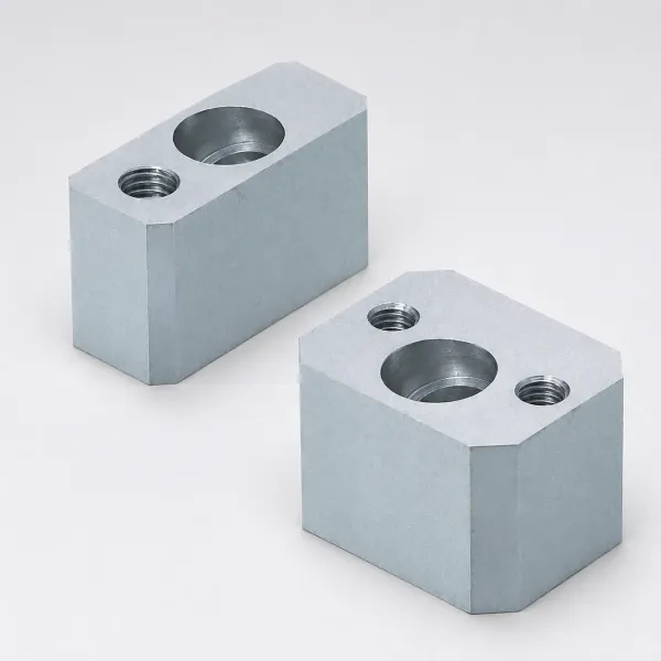
Uniform roughness across the masked area. A common requirement is that Ra varies by no more than 20% across the face, with no polished islands inside a textured field. Two zones at Ra 0.3 µm and Ra 0.6 µm will etch to two visibly different shades.
No white layer, no weld repair in the grain area. The recast layer must be fully removed before etching, because a 2 to 10 µm layer left under a grain shows as a blotchy patch on the molded part. Any weld that was dressed but not stress-relieved etches deeper than the parent steel, and the spot is unrecoverable once the grain is in.
No residual polishing stress. Over-polished areas with heavy pressure develop surface stress that shows as orange peel after etching, the same defect the bench fights on gloss surfaces above SPI B2 at Ra 0.2 µm. Light, sequenced passes from 600 to 1200 grit avoid it.
A base polish at or finer than the grade needs. Fine grain near 0.015 mm needs a substrate at Ra 0.2 µm or better. Coarse grain near 0.05 mm will accept a substrate at Ra 0.4 to 0.8 µm, which is where a clean finish EDM plus a light stone pass lands. Matching the two saves bench hours that buy nothing.
Clean, dry, and labelled. Oil, rust inhibitor and fingerprints can all interfere with masking and etch. Parts should arrive degreased, with the textured faces marked on a sketch or on the part itself, and with the approved plaque number written on the paperwork. DieStrike project engineers confirm these points at DFM, with feedback inside 24 hours, because a substrate question caught before the burn is free and caught after the etch is a strip and re-etch cycle.
Specifying Both on One Drawing
A working finish spec on a mold drawing does not need to be long. 4 line items per graded face are enough: the surface, the roughness, the method and the acceptance evidence. Most disputes come from one note covering the whole tool.
Zone the cavity first. Mark cosmetic faces, non-cosmetic faces, shut-offs, sealing lands and areas that must stay sharp for fit. Each zone gets its own line. A connector housing might run SPI B2 on the visible shell, SPI C3 on the interior ribs, and no finish call-out at all on the bore that holds the core pin.
Then write each line with four parts. One, the SPI grade or the texture class. Two, the Ra limit with a number and a unit, for example Ra 0.2 µm max. Three, the method constraint, for example "no EDM on cosmetic faces" or "EDM permitted, then stoned to Ra 0.8 µm". Four, the acceptance evidence, for example "compared against plaque MT-11020 under D65 light" or "Ra verified on 0.8 mm cutoff at three points".
State the polish direction and the corner rules. A single-direction polish against the flow direction is worth writing down, because a cross-polished surface releases differently. So is a note that edges and shut-offs must not be broken by polishing, with a maximum allowable radius wash-out, usually 0.02 to 0.05 mm depending on the sealing function.
Give the EDM cell its own line. If cosmetic faces must not see a spark cut, say so explicitly. If they may, give the last EDM step a target such as "finish EDM to Ra 0.4 to 0.8 µm, then stone". That one line prevents the most expensive version of this whole problem, which is a polished and approved cavity that gets re-sparked to fix a weld line two days before sampling.
DieStrike builds to ±0.005 mm on mold dimensions and ±0.002 mm on part geometry, with cavities heat treated to HRC 62 where the resin demands it. Injection molds and stamping dies both run on a 2 to 5 week lead time, so a finish question that arrives late lands directly on the ship date. Writing the two finish systems onto one drawing at RFQ stage costs an hour of engineering time.
Acceptance: Plaques vs Roughness Testers
Acceptance is where a good specification either holds or falls apart, and it takes 2 different instruments because the steel and the molded part are judged on different evidence. The steel needs a number and the molded part needs a look, so a report that carries only one of the two leaves the other open to opinion at the trial.
Visual plaques govern grain and gloss. A plaque is a molded reference standard, matched to a resin and colour, held by both the buyer and the tool shop. Inspection is done under a defined light, often D65, at a set viewing distance, usually 0.5 to 1 m, with the part rotated to catch reflections. On textured parts the practical acceptance band for a matte interior grain is roughly 3 to 5 gloss units at 60 degrees. Plaques catch shade, density and direction, which is exactly what a stylus cannot describe.
Roughness instruments govern the steel. A contact profilometer with a 0.8 mm cutoff reads Ra and Rz on the polished and pre-etch faces. Take at least three readings per graded face, positioned away from edges and ribs so the stylus does not ride a wall. A reading of Ra 0.35 µm on a face specified at Ra 0.2 µm max is a real rejection, and it is the kind of finding that must be raised before the etch, not after.
Optical instruments cover what a stylus cannot reach. White-light or focus-variation instruments read crater fields and fine grain without dragging a tip across them, which makes them the better tool on a textured or re-melted surface. They also produce Sa and Sz values on an areal basis over a typical 2 by 2 mm measuring field, and a shop comparing a returned tool against its original report can use those numbers to prove the surface has not drifted.
Gloss measurement closes the loop on the molded part. A 60 degree gloss meter reading on a production part is the cheapest end-of-line check available, and it turns a subjective "looks different" into a number two people can argue about with evidence. Keep the meter, the geometry and the resin batch the same between runs, or the number moves for reasons that have nothing to do with the tool.
A coupon plate saves the argument. Before a cosmetic cavity is burned, run a coupon of the same steel through the same EDM, polish and etch route. The coupon costs 2 to 4 hours of shop time, it carries the same hardness, and it shows the final surface before the tool is committed. If the coupon shows ghosting from the spark pattern, the fix is a polish step on the coupon, not a strip and re-etch on a finished cavity.
Cost and Lead Time Impact
Finish decisions land in the quote as machine hours, bench hours and outside processing days, and each one can be moved earlier at low cost or later at high cost. The pattern is consistent across tools. A finish call-out settled at RFQ stage costs an hour of engineering time. The same call-out settled after the etch adds 2 to 4 weeks to the ship date.
EDM time scales with the finish target. A roughing burn that clears a pocket at Ra 3.2 to 6.3 µm is fast and cheap in electrode wear. Each step toward Ra 0.4 µm adds skim passes, low-current settings and orbit cycles, and a mirror-class route through EDM is slow and hard on electrodes. On many cavities the practical route is a semi-finish burn at Ra 1.6 µm plus bench work, because that combination costs less than an EDM route to Ra 0.2 µm.
Bench hours are the largest variable. A C-class finish takes 1 to 4 hours on a small insert. A B-class finish takes 10 to 25 hours. A mirror finish takes 30 to 60 hours, and the hours climb sharply with rib count, depth and inaccessible corners. Those hours are quoted as a line item on any honest tool quote, so a specification written at RFQ stage simply prices the finish before the mold is cut instead of after.
Outside etch adds calendar days, not just cost. Photo-etch processing typically runs 5 to 10 business days door to door once the box arrives, and a strip and re-etch runs 2 to 4 weeks because the tool travels twice and the masking is rebuilt. A re-etch on hardened steel also costs roughly 15% to 30% of the original texture line.
The failure cases have known price tags. Re-sparking a hardened insert to fix a weld line costs 4 to 10 hours of machine time and electrode wear, plus a trip back through the bench. Re-polishing after an uneven etch runs 8 to 20 hours. Either event pushes a tool that was tracking to a 2 to 5 week lead time into a delay that shows up on the sampling date. DieStrike checks finish call-outs at DFM, with feedback inside 24 hours, because the cheapest change is the one made before the first electrode is burned.
FAQ: EDM Finish and SPI Texture
Q1. Can I etch a texture straight over an EDM finish without polishing first?
Sometimes. The etch depth must be at least three times the crater depth. A coarse grain at 0.05 mm will hide a finish cut at Ra 1.6 µm with a crater depth near 6 to 12 µm. A fine grain near 0.015 mm will not hide that surface, and the spark pattern will ghost through on the molded part. The recast layer must be removed in either case, so a light stone pass is almost always needed.
Q2. Does an SPI grade replace an EDM finish call-out?
No. The two lines control different things. The SPI grade or texture class controls what the customer sees on the part. The EDM line controls the substrate, the spark finish allowed on non-cosmetic faces, and the roughness the bench inherits. Drop the EDM line and the shop is free to leave Ra 3.2 µm under a polish target of Ra 0.2 µm, which adds 20 to 40 bench hours nobody quoted.
Q3. How much stock should I leave for a mirror finish after EDM?
Plan on 0.05 mm for SPI A2 at Ra 0.025 µm, and add 0.01 mm for deep ribs or blind pockets. That allowance covers the 2 to 10 µm recast layer plus the grade work. Expect 30 to 60 bench hours on a hardened insert of roughly 100 by 100 by 50 mm, and more if the cavity has sharp internal corners that limit stone access.
Q4. Which VDI or Charmilles number goes with SPI C1?
Ra 0.8 µm sits near Charmilles 18 and near the VDI 3400 grade 37 in the commonly used charts, and SPI C1 is also Ra 0.8 µm. Never rely on the scale number alone. Write the Ra value with its unit next to the scale number, because VDI and Charmilles charts drift between machine builders and texture vendors.
Q5. How do I inspect a textured surface if a profilometer cannot read the grain?
Use a plaque for grain and gloss, and use a gloss meter at 60 degrees on the molded part for a number. Reserve the profilometer for the polished faces and for the pre-etch substrate, where a Ra limit is meaningful. For disputed cases, an optical 3D instrument gives areal Sa and Sz values on the texture without touching it. A coupon plate run through the same route is the strongest evidence of all.
The Bottom Line
EDM finish and SPI texture meet on the same steel, and the gap between them is where tools lose days. Name both systems on the drawing, put an Ra number beside every scale number, and set stock at 0.02 to 0.05 mm after the last burn. DieStrike cuts, burns, and finishes precision molds for connector, automotive, and consumer electronics programs, with finish specs confirmed at DFM before steel is cut. Send your drawings and finish call-outs through the contact page for a review against these rules.
KEEP READING
Related Reading
Mold Polishing Guide: From Ra 3.2 to SPI A1
SPI A1 to D3 grades, the 240 to 3000 grit diamond sequence, and steel polishability from P20 at 28 HRC to S136 at 52 HRC.
Read articleArticleHow to Specify Mold Texture: SPI, VDI and Grain Matching
Etch depth 0.015 to 0.08 mm, VDI 3400 grades, draft of 0.5 to 1.5 degrees per side, and the 7 line texture spec sheet.
Read articleArticleSinker EDM vs Wire EDM: Which Cuts Your Mold
When to burn a cavity with sinker EDM and when to cut it with wire. Accuracy, electrode cost and surface finish compared.
Read articleServiceMold Trial & T1 Sampling
T0 to Tf sampling milestones with dimensional reports, gloss checks and first-article sign-off before the mold ships.
Read articleNEXT STEP
Ready to Start Your Mold?
Send us your element dimensions or part numbers — our team responds within 24 hours with pricing and lead time.

Written by
Ray ChanMold Buyer's Guide Author · Precision Mold Manufacturing Specialist. Ray helps global importers, distributors and OEMs source factory-direct molds and mold parts.